
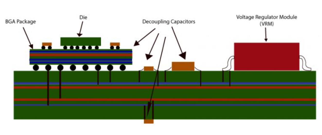
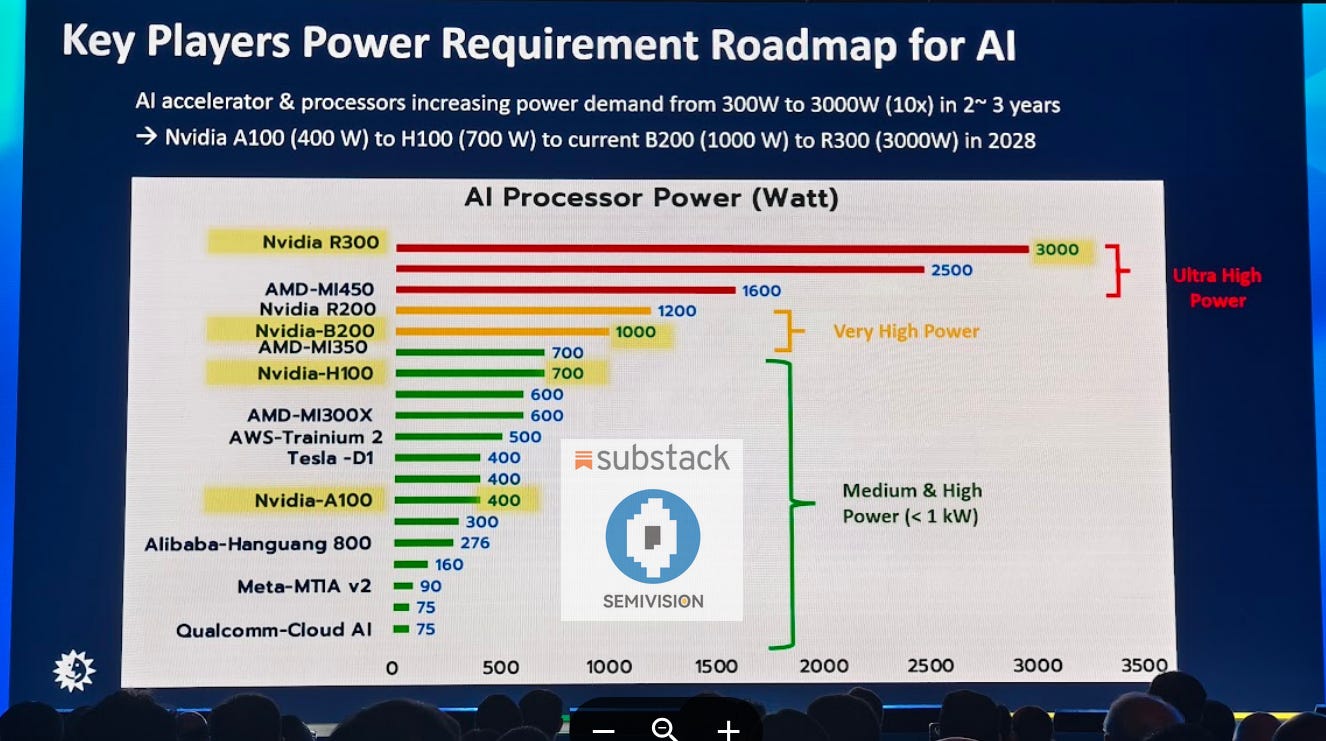
As the complexity and power demands of AI chip designs continue to escalate, Power Delivery Networks (PDNs) and thermal management have emerged as unavoidable core challenges for the industry. Traditional power delivery through PCBs or ABF substrates is becoming increasingly inadequate due to long power paths and high parasitic inductance, leading to IR drops and transient voltage droops. With single GPUs now requiring over 1000A of current, these legacy approaches are approaching their limits.
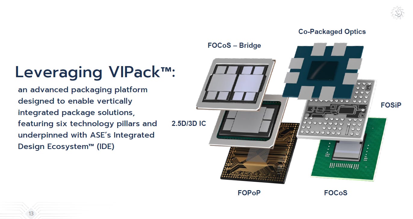
To address these challenges, foundries and OSAT (Outsourced Semiconductor Assembly and Test) providers are actively proposing solutions across different integration levels. For instance, Marvell has introduced the PIVR (Package-Integrated Voltage Regulator), embedding the VRM directly into the package to shorten the power path and reduce PDN impedance, enabling faster voltage response. ASE, through its VIPack and FOCoS-Bridge (with TSV) platforms, is optimizing PDN, signal interconnects, and thermal performance simultaneously—especially for Chiplet + HBM packages that demand high bandwidth and I/O, enabling reduced power loss without compromising performance.
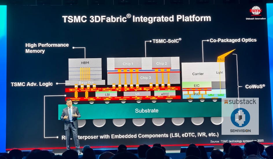
TSMC, on the other hand, is pursuing a more diversified integration strategy. In its CoWoS-L platform, TSMC embeds IVRs and eDTCs (embedded Deep Trench Capacitors) to enhance on-die decoupling density and power stability, while also developing BSPDN (Backside Power Delivery Network) to physically separate power and signal layers. This reduces voltage drop and frees up valuable front-side routing resources. TSMC is also pioneering thermal co-design, incorporating Direct Liquid Cooling (DLC), microchannel technologies, and exploring new materials for TIM (Thermal Interface Material) and underfill, with the goal of enabling reliable operation of kilowatt-class AI chips.
Under these trends, NVIDIA and other hyperscalers are beginning to view materials as a critical pillar in AI chip and system design, actively pushing the supply chain to explore diversified material options. Among these, Silicon Carbide (SiC) has suddenly become a focal point of attention.
Proven over the past three decades in the power electronics sector, SiC has emerged as a star material due to its wide bandgap (WBG), high thermal conductivity, high breakdown field strength, excellent thermal stability, and high Young’s modulus. It has already been successfully commercialized in electric vehicle inverters, industrial power modules, and high-voltage grid systems. Now, with the explosive growth in AI computing demand, SiC’s role is rapidly expanding into advanced packaging and heterogeneous integration.
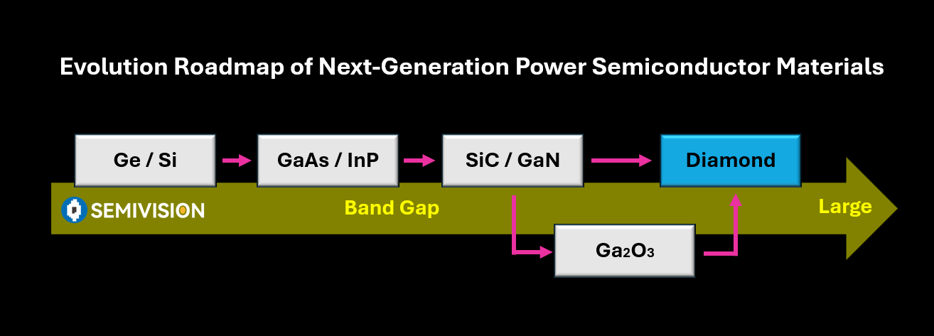
SiC holds the potential to become the substrate material for high-voltage ICs (HVICs) and on-chip power delivery, supporting developments in BSPDN and IVR architectures. It also shows great promise as an optical interposer, offering a thermally conductive, low-loss platform for silicon photonics (SiPh) and lithium niobate (LN) modulators. Furthermore, its high rigidity and thermal conductivity are beneficial for large-area 3D stacking of Chiplets and HBM, helping reduce package warpage while enhancing mechanical reliability.
These unique properties position SiC as a key material linking PDN, thermal, and optical interconnect domains, driving strong investment and development efforts from the Taiwanese supply chain. The goal: to establish new industrial advantages in the age of AI and HPC.
Driven by generative AI and large-scale model training, companies like NVIDIA, AMD, Google, and AWS are successively launching ultra-large-scale GPUs and ASICs priced at tens of thousands of dollars each. These chips contain hundreds of billions or even trillions of transistors, with power consumption often exceeding 1 kW—placing demands on thermal management, power delivery, and signal interconnects that far exceed those of traditional HPC and server chips.
This exponential growth has revealed three critical bottlenecks in process and packaging technologies:
Thermal Challenges:
AI chips now generate heat flux densities that push conventional thermal interface and substrate materials to their limits. Whether it's silicon interposers, glass cores, or ABF substrates, existing materials are increasingly unable to meet the thermal conductivity and long-term reliability requirements.
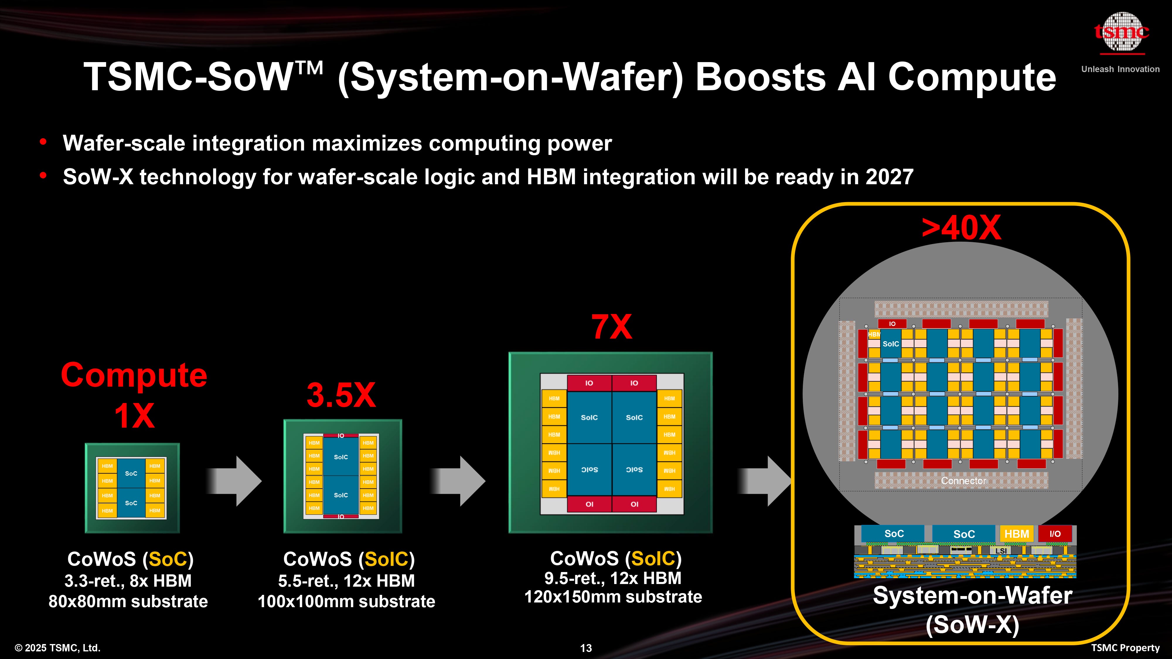
This challenge also extends to optical components such as lasers and modulators, whose performance is highly temperature-sensitive—minor thermal fluctuations can lead to bandwidth degradation and system-level errors. To tackle these thermal limitations, TSMC is focusing on evolving its CoWoS-L platform through reticle scaling, expanding package sizes from 5.5X to 9.5X to support higher integration density. TSMC is also advancing its SoW-X (System on Wafer) architecture to further enhance 3DFabric integration, while exploring CoPoS (Chip on Panel on Substrate) and other ultra-large-area packaging technologies to open up new possibilities for 3D integration and heterogeneous packaging.
These strategies reflect TSMC’s comprehensive response to AI/HPC power and thermal demands—advancing across materials, architectures, and process nodes.
Power Delivery Bottlenecks:
As AI chip power demands rise, power delivery through packaging layers or PCBs alone is no longer sufficient. Backside Power Delivery Networks (BSPDNs), Integrated Voltage Regulators (IVRs), and vertical power delivery architectures are becoming essential. These approaches require substrate materials with high voltage endurance and low-resistance conduction capabilities.
Electro-Optical Integration Demands:
To overcome the physical limits of SerDes bandwidth, optical interconnects have become a critical direction for AI chip architecture. Efficient integration of silicon photonics (SiPh) components, germanium photodetectors, and lithium niobate (LiNbO₃, LN) modulators with logic chips and high-bandwidth memory is essential for advancing 3D packaging and heterogeneous integration. According to SemiVision, current SerDes technologies are hitting a ceiling at 448G, and breaking through this limit will require next-generation photonic materials and platforms. TSMC is now actively developing next-gen silicon photonics to meet the extreme bandwidth, latency, and power efficiency requirements of AI/HPC systems—while tightly integrating this with advanced packaging, forming a new electro-optical architecture.
As artificial intelligence (AI) and high-performance computing (HPC) drive explosive demand for memory bandwidth, chip interconnect density, and power-thermal management, the traditional monolithic silicon SoC architecture and the size limits of silicon interposers have increasingly become bottlenecks in system design. TSMC’s 3DFabric strategy addresses these challenges through diversified packaging solutions such as InFO, WMCM, and SoW, with the CoWoS family at the forefront—focusing on how to integrate high I/O density, low latency, efficient heat dissipation, and robust reliability within advanced packages.
In CoWoS-S, the use of silicon interposers combined with TSVs provides exceptional signal and power integrity. However, once the interposer size surpasses the reticle boundary, yield and mechanical fragility risks rise sharply. To mitigate these limitations, CoWoS-R introduces an RDL-based organic interposer architecture, leveraging polyimide/polymer dielectrics with fine copper routing to redistribute signals and power. This not only sustains strong electrical performance but also alleviates thermal expansion mismatches and mechanical stress. Building on this, CoWoS-L integrates local silicon interconnect dies with higher-order RDL structures, enabling ultra-large interposers and more complex chiplet-HBM integration for future AI/HPC designs.
Recently, breakthroughs in materials have emerged as a potential game-changer. TSMC is exploring the use of single-crystal silicon carbide (SiC) as an interposer or substrate, aiming to capitalize on SiC’s superior thermal conductivity and mechanical robustness to enhance heat dissipation and reliability, while overcoming the inherent size and material limitations of silicon interposers. At the same time, panel- and PCB-level packaging approaches such as CoWoP and CoPoS are surfacing as complementary or competitive alternatives to CoWoS, particularly for large-form-factor, cost-sensitive markets that still demand high performance.
This article will systematically examine the role of RDL in the CoWoS family with respect to power integrity, signal integrity, reliability, and stress control, assess the feasibility of SiC as an interposer or substrate, and evaluate whether emerging form factors such as CoPoS and CoWoP may redefine the trajectory of TSMC’s 3DFabric ecosystem.